IBM’s new chip-stacking technique
IBM said on Wednesday it will be able to make
microchips faster and more energy efficient by stacking components on top of
each other.
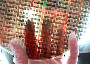
A “thinned” wafer ready to be joined to another
IBM said on Wednesday it will be able to make microchips faster and more energy efficient by stacking components on top of each other, a breakthrough that cuts the distance an electrical signal needs to travel.
The technique works by drilling tiny holes through a wafer of silicon and filling them with metal. Components such as memory can then be stacked on top of the main part of the chip, eliminating the need for wires stretching out to the sides.
IBM likened the method to replacing a sprawling airport parking lot with a multi-storied garage right next to the terminal. Like people walking from the garage to the terminal, electrical signals do not have to travel as far in a chip with stacked components.
IBM will use the method to make power management chips for wireless devices later this year, allowing them to use 40 percent less power than previous versions, Lisa Su said in an interview.
They plan to follow-on with processors for larger devices. An obvious example why a solid program of R&D keeps the best tech companies in business seemingly forever.
More on the technology over here.
Posted: Thu - April 12, 2007 at 08:25 AM